
Statement of Work for
SVS Custom Electronics PCB Fabrication & Assembly
Page 1 of 14
TABLE OF CONTENTS
1. Introduction .......................................................................................................................................... 2
2. Scope .................................................................................................................................................... 2
3. Government Furnished Equipment ....................................................................................................... 2
4. References ............................................................................................................................................ 3
4.1 Requirements ................................................................................................................................. 3
4.2 Procedures and Forms ................................................................................................................... 3
4.3 National/International Standards ................................................................................................... 3
5. Task 1- Project Management ................................................................................................................ 4
5.2 Task 2 – Inspection Plan ................................................................................................................ 4
5.3 Task 3 – Quality Plan .................................................................................................................... 5
5.4 Task 4 – Manufacturing Readiness Review .................................................................................. 5
5.5 Task 5 – PCB Materials Procurement and Production .................................................................. 5
5.6 Task 6 – Testing ............................................................................................................................ 6
5.7 Task 7 – Documentation ................................................................................................................ 7
5.8 Task 8 – Manufacturing Dossier ................................................................................................... 7
5.9 Task 9 – Combined PCB Shipment ............................................................................................... 8
5.10 Task 10 – Data Management ......................................................................................................... 8
6. Quality Assurance ................................................................................................................................. 9
7. Deliverables ........................................................................................................................................ 13
7.1 Hardware ..................................................................................................................................... 13
7.2 Documentation ............................................................................................................................ 14

Statement of Work for
SVS Custom Electronics PCB Fabrication & Assembly
Page 2 of 14
1. INTRODUCTION
ITER is an international research project with a programmatic goal of demonstrating the scientific and
technological feasibility of fusion energy for peaceful purposes. The European Union is the host party for
the ITER facility which is being constructed in Cadarache, France. Governing regulations, codes, and
standards for the design and construction of all ITER components are determined by the European Union
and France. The US portion of ITER is managed by the US ITER Project Office (USIPO) which is
hosted by Oak Ridge National Laboratory (ORNL) under contract with UT-Battelle (hereinafter referred
to as the “Company”), and located in Oak Ridge, Tennessee.
Five custom Printed Circuit Boards (PCBs) are required for the Service Vacuum System (SVS)
electronics: Analog Front End (AFE), Front End Acquisition & Control (FEAC), Front End Acquisition
& Control Regulator Daughterboard (FEAC-RDB), Profinet digital interface (PDI), and Power
Management (PM). As shown in Figure 1, the Wall Mounted Cubicle (WMC) houses the AFE, the
FEAC (with associated FEAC-RDB), and the PM, while the corner cubicle will house the PDI board.
The AFE board and FEAC boards shall be mounted together with the FEAC boards stacked on top of the
AFE board with a specific offset within the WMC.
2. SCOPE
The scope of this Statement of Work (SOW) includes fabrication, assembly, inspection and testing of
PCB boards that fulfills the requirements of the Technical Specification [1]. This Statement of Work
(SOW) defines the activities to be performed by the Seller for the fabrication, testing, configure,
validation/qualification, and packing of the Printed Circuit Boards.
The Seller is assumed to be an expert in all aspects of circuit board production and assembly and shall
not use this specification as a basis for providing product that is below normal standards of production in
any manner. The Seller shall remain responsible to deliver populated PCBs in compliance with the
technical specifications herein and with industry standard quality and workmanship.
3. GOVERNMENT FURNISHED EQUIPMENT
The Company will provide Specialized Integrated Circuits as Government Furnished Equipment (GFE)
equipment that is owned and serialized by the government and delivered to or made available to the
Seller. The Seller while in possession of the property on the executed contract with the Company
acknowledges and agrees to accept custody and safeguard the property during the period that the contract
is in effect or that the Seller completes the project.
The unique properties and cost of the GFE makes it necessary to safeguard it from any damage or loss.
The Seller will provide fireproof safe/room that is recognized as UL Class 350 – 2hr [16] (formerly Class
B) and Controlled access for storage of GFE.
In addition to the terms and conditions set forth in the contract executed between the Seller and the
Company, the Seller agrees to:

Statement of Work for
SVS Custom Electronics PCB Fabrication & Assembly
Page 3 of 14
1. Perform and report an inventory of the assigned GFE upon request from the Company. The
inventory will be required to be reported on during the Fiscal Year (FY) as a DOE requirement.
The Company custodian will also be required to confirm those items in Seller inventory annually
or until the project’s completion.
2. Return the property to the Company or their designee upon request by the Company or their
designee.
4. REFERENCES
Documents are provided to supplement this Statement of Work to the extent involved in defining
requirements necessary to complete. These documents include company documentation and
recognized national standards:
Unless otherwise specified, the correct revisions of national and international standards, US ITER technical
documents, drawings, specifications, and other job-related documents will be identified on the “Current
Reference List for SVS Fabrication of Custom Electronics” (EDRM 804b65d7) provided at the time of
award and as reference documents are updated.
4.1 Requirements
[1] Technical Specification for Service Vacuum System Custom Electronics Boards, 804b64b6
4.2 Procedures and Forms
[2] Requirements for Producing a Quality Plan, ITER_D_22MFMW
[3] Quality Plan Template for Suppliers and Subcontractors, 8043657d
[4] Requirements for Producing an Inspection Plan, ITER_D_22MDZD
[5] Inspection Plan Template, 80411682
[6] Deviation Request Procedure, 803fee84
[7] Deviation Request Form, 803f59df
[8] Nonconformance Reports Procedure, 803f913f
[9] Non-Conformance Report Form, 8043b412
[10] Contractor Release Note Procedure, 8041191f
[11] Contractor Release Note Form, 803f4967
[12] Manufacturing Readiness Review Procedure, 804a455c
4.3 National/International Standards
[13] Electrostatics - Part 5-1: Protection of electronic devices from electrostatic phenomena -
General requirements, IEC 61340-5-1 & 2
[14] Qualification and Performance Specification for Rigid Printed Boards, IPC-6012D
[15] Acceptability of Printed Boards, IPC-A-600F.
[16] Underwriters Laboratories UL Class 350-2hr: Safes Rating and Performance Requirements
Statement of Work for
SVS Custom Electronics PCB Fabrication & Assembly
Page 4 of 14
5. TASK 1- PROJECT MANAGEMENT
5.1.1 Project Management
The Seller will designate an official single Point of Contact (POC) to work with the Company’s
Technical Project Officer (TPO) and Procurement Officer (PO). Technical issues will be discussed with
the Company’s TPO. Subcontract administration issues will be discussed with the Company’s PO.
Changes to the Statement of Work (SOW) or technical specification can be officially authorized only by
the Company’s PO. The Seller will prepare a project plan that integrates each element of subcontract
management into a concise written document. The project plan will identify the Seller’s key personnel in
this project and describe their individual roles and responsibilities.
The Seller will prepare a schedule, which will identify, at a minimum, all work tasks, meetings, progress
reports to the TPO, hold points, key milestones, and dates for deliverables. The project schedule will be
kept up to date by the Seller when changes occur.
5.1.2 Kickoff Meeting
The Seller will arrange a project kickoff meeting, which will be scheduled at a mutually agreeable time
and place as soon as practicable after award of contract, but not before the draft schedule (section 5.1.1)
and draft quality plan (section 6.1.2) are submitted by the POC to the TPO.
The kickoff meeting will include the POC, and Seller’s other project management and engineering team
participants as requested by the Company. The primary purpose of the meeting is to confirm that the
meeting participants understand the terms and conditions of the subcontract, the SOW, and the technical
specification.
The Seller will prepare written kickoff meeting minutes that document the agreements and commitments
resulting from the kickoff meeting discussions. The Seller will send the minutes to the TPO for review
and approval within ten working days after the meeting.
5.1.3 Progress Meetings
Technical and progress teleconferences and meetings between the Company and Seller will be
held at a scheduled time and location mutually agreeable to the TPO and POC. The discussions
will include the Seller’s progress, potential problems, resources, technical issues, contractual
issues, manufacturability issues, and testing results. The Seller will prepare and send minutes of
the teleconferences and meetings to the TPO for review and approval within ten working days
after the meeting.
5.2 Task 2 – Inspection Plan
The Seller will develop an Inspection Plan (IP) in accordance with section 6.1.3 and submit the
IP for approval prior to manufacturing.

Statement of Work for
SVS Custom Electronics PCB Fabrication & Assembly
Page 5 of 14
5.3 Task 3 – Quality Plan
5.3.1 Quality Assurance
The Seller will prepare and submit a Quality Plan in accordance with section 6.1.2.
The Seller will provide an ESD program in accordance with IEC 61340-5-1 & 2 [13], as part of the
Quality Plan, for safe handling and fabrication of the PCBs. The standard covers the requirements
necessary to design, establish, and implement an ESD control program to protect electrical or electronic
parts, assemblies, and equipment susceptible to ESD damage from human interaction with parts and
assemblies.
Technical Recommendations
• Plan shall include items such as grounding, personal grounding, protected areas, packaging,
labeling, equipment, and handling.
• At a minimum wrist straps and anti-static mats
5.4 Task 4 – Manufacturing Readiness Review
The Seller will provide manufacturing and test procedures for approval from US-IPO. Approval of these
documents is a prerequisite to start manufacturing.[12]
The purpose of this procedure is to define the process for conducting the Manufacturing Readiness
Review (MRR). The MRR is employed to confirm the readiness of a manufacturer to produce systems.
Ensure MRR milestones are included in the planning/schedule for the WBS.
5.5 Task 5 – PCB Materials Procurement and Production
Following Company approval of the inspection plan, the Seller will fabricate, assemble, inspect, and test
PCBs in accordance with this SOW and the Technical Specification [1]. The Seller will then construct
the PCB boards with the given fabrication files per a Class III build per IPC 6012D [14] and IPC-A-600F
[15]. Populate PCB boards with the circuit components.
The Seller will be solely responsible for the procurement of materials and components apart from the
specific equipment furnished by the Company (GFE), fabrication and assembly, inspection, examination,
cleaning, and preparation of PCB boards for shipping and delivery.
The Seller will document production activities using manufacturing dossier developed in section 5.8.
5.5.1 Component Procurement
Once the MRR is agreed upon, the Seller is to procure enough materials to furnish the complete order of
PCB’s but only obtaining enough resistors as necessary for the initial three boards required and outlined
below in section 5.6.1 for Seller and Company Testing.
Using the data provided by the Company for each Printed Circuit Board (PCB) the Seller will
manufacture a total specified number of boards defined in section 7.1 to the Companies satisfaction.
Statement of Work for
SVS Custom Electronics PCB Fabrication & Assembly
Page 6 of 14
5.5.2 Production
The Seller will use the Fabrication file package provided to initially produce First Article PCB boards,
three (3) Quantity of each AFE, FEAC, FEAC-DB, PM, and PDI.
Once the custom electronics have been fabricated, tested, and accepted by the Company, the Seller will
produce the required remaining quantity of units. All units must be produced to the same quality
standards and specifications as the accepted First Articles.
After acceptance of First Article Testing a conformal coating will be applied to all PCB’s. The Seller will
specify to the Company a best fit application utilizing the Company’s environmental and material
criteria.
5.6 Task 6 – Testing
5.6.1 First Article Testing
The Seller will test the First Article boards and send them to the Company for functional testing. The
Company will clear the further production based on the outcome of the test or require the Seller to make
necessary changes before the production as deemed necessary.
5.6.2 Seller Testing
The Seller’s required testing is outlined in the Technical Specification [1].
Incorporated in the PCB design are PCB test points that are used by the Seller to monitor the state of the
circuitry or to inject test signals. These are located throughout the board and at various stages in board
construction, they are primarily used to verify electrical connectivity. The fabrication package includes
the netlist that highlights these test points to be used in the electrical testing of the fabricated boards.
5.6.3 Test Results
The Seller will make immediately available the results of the First Article Testing outlined in the
technical specification, as a test report.
The Seller will provide updates to drawings and BOM with the supply of the PCB boards if changes are
required for manufacturability.
5.6.4 Company Testing
The Company will perform the functional testing of First Article boards as well as all Production run
boards. However, this does not exclude the Seller from doing the testing from previous section or
performance responsibility.
The Company will require a minimum of twenty-one (21) working days from receipt to test and examine
the boards.
Statement of Work for
SVS Custom Electronics PCB Fabrication & Assembly
Page 7 of 14
5.7 Task 7 – Documentation
5.7.1 Contractor Release Note
Each delivery to the ITER site will have a Contractor Release Note (see section 6.1.4).
5.7.2 Certificate of Conformity
The Seller will prepare a Certificate of Conformity for the supplied hardware. The Certificate of
Conformity will state that the items meet all requirements defined in the technical documentation [1] and
this statement of work. The designated POC will submit the completed Certificate of Conformity to the
TPO. Once approved, the Certificate of Conformity will be returned by the USIPO to the Seller for
inclusion in the Manufacturing Dossier.
The Seller may use any suitable format for the Certificate of Conformity. At a minimum, the Certificate
of Conformity will include:
• Manufacturer’s details (name, address, etc.)
• Item identification details (model, serial number, etc.)
• Declaration that the equipment meets the applicable requirements (specifically list requirements
documents)
• Any standards the item complies with
• Signature of Sellers’s authorized representative.
5.8 Task 8 – Manufacturing Dossier
The Seller will produce a Manufacturing Dossier at the completion of Task 3. The dossier will include all
records that provide documentary evidence that the activities associated with the manufacture of the
boards meet specified design, performance, and quality requirements.
All records must be sufficient to provide objective evidence that the approved design is implemented in
the manufactured product.
The Manufacturing Dossier will have a Table of Contents and sequentially numbered pages and will be
legible and traceable to associated items and activities and accurately reflect the work accomplished or
information required.
Manufacturing Dossier Contents (at a minimum)
• General description of the boards and components used for construction.
• Test and inspection reports as required by Technical Specification & Inspection Plan
• Material Inspection Reports
• Approved Deviation Requests, as necessary
• Non-Conformance Reports, as necessary

Statement of Work for
SVS Custom Electronics PCB Fabrication & Assembly
Page 8 of 14
• Manufacturing Reports
• Contractor Release Note
• Certificate of Conformance
• Receiving, Handling, and Storage Procedures and/or Instructions
• As-built Layout Files & Bill of Materials, as necessary
5.9 Task 9 – Combined PCB Shipment
Deliver the three (3) boards of each type for testing by the company outlined in Task 4. Once authorized
the remainder of the order will be shipped to the with same packaging specification to the same location
outlined to follow.
The packaging shall prevent damage to the PCB edges and corners as well as the components. The
following shall be used in the packaging:
• Packaging Materials for ESD Sensitive Items will apply: This standard defines the packaging
properties needed to protect electrostatic discharge susceptible (ESDS) electronic items through
all phases of production, transport, and storage.
• Vacuum sealed moisture barrier bag.
• Humidity indicator card
• Desiccant compatible with PCB and finish
• Suitable bubble wrap, as required.
By default, the shipment shall be delivered to the following address:
UT Battelle, LLC for the Dept. of Energy
c/o Oak Ridge National Laboratory
US ITER Project Office
1 Bethel Valley Road, Bldg. 7120
Oak Ridge, TN 37830
The Company may decide to change the delivery address, if necessary, at the later time.
5.10 Task 10 – Data Management
5.10.1 Language and Units of Measure
All documentation will be in English, and all dimensions and parameters will be reported in metric units
except for trade size components that are specified in other units. Dual English/metric units are
acceptable.
5.10.2 Electronic Copy Format
The Seller will provide electronic copies of all documentation. The electronic copies will be in
searchable (not scanned) Portable Document Format (PDF).
Statement of Work for
SVS Custom Electronics PCB Fabrication & Assembly
Page 9 of 14
5.10.3 Correspondence
Electronic documents will be supplied to the Company using e-mail or a USB storage device. Any
documentation supplied by the Seller to the Company via email will be sent to the TPO. Documentation
supplied by the Company to the Seller will be sent to the POC, who will be responsible for distributing it
to appropriate staff.
6. QUALITY ASSURANCE
6.1.1 Quality Program
The Seller’s Quality Program shall be implemented and sufficient to ensure that the quality of items
produced, or services provided will meet all the requirements as stated in this document and as
contracted. The Seller must produce the items or services in accordance with their quality assurance
program as identified in their subcontract with the Company. Changes to the program that could affect
the items or services must be approved by the Company in advance.
Seller’s QA program shall include QA record receipt controls, which provide a method for identifying
records received, receipt and inspection of incoming records, record retention, and transmittal of records.
6.1.2 Quality Plan
ITER requires that a Quality Plan be prepared by the Seller that incorporates the requirements per
Requirements for Producing a Quality Plan [2], specifically for the subcontract, identifying how they
will fulfill the specific subcontract requirements.
NOTE: This plan is in addition to the pre-established Quality Program, Management System
Description, Quality Manual, or equivalent of the Seller’s organization as detailed in
paragraph 6.1.1.
Work on the subcontract may not begin until notice is received that the Quality Plan is approved by the
Company.
The requirement for a subcontract-specific Quality Plan per Requirements for Producing a Quality Plan
[2] shall be flowed down contractually from the Seller to the Sellers suppliers and subcontractors, unless
the requirement is waived in writing on a case-by-case basis by the Company. [Example: COTS items
(not modified for ITER)].
A revised Quality Plan (at all levels) shall be subject to the same approval and acceptance procedure as
the original Quality Plan. In case of revision, work should continue in accordance with the current
approved Quality Plan until the revised Quality Plan is accepted.
A standard template [3] is available from the Company for documenting the contract-specific Quality
Plan, but the Seller may propose to use their own equivalent format.
The quality plan shall cover the ESD program and storage & inventory management of GFE material.

Statement of Work for
SVS Custom Electronics PCB Fabrication & Assembly
Page 10 of 14
6.1.3 Inspection Plan (IP)
Sellers who contract to manufacture items shall prepare an Inspection Plan—specific to the production of
the item(s) described in the contract—as prescribed by Requirements for Producing an Inspection Plan
[4] and submit it for approval.
A standard template [5] is available from the Company for documenting the IP. A Seller may propose to
use its own equivalent format; however, it must be accepted by the IO Quality Division.
Manufacturing may not begin until notice is received that the IP has been approved by the Company.
The requirement for an IP shall be flowed down contractually from the Seller to the Seller’s suppliers
and subcontractors unless the requirement is waived in writing on a case-by-case basis by the Company.
Examples not requiring an IP:
1) COTS items (not modified for ITER)
2) Research & development activities
3) Supply of services
The IP will list the sequence of manufacturing operations encompassing the whole scope of the
subcontract and range from review of drawings, verification of materials, manufacture, inspection, and
test to delivery. It will be used to monitor quality control and acceptance tests.
The Company will add any Company intervention points and send the IP to the IO for acceptance and
mark-up of any IO intervention points, before returning it “approved” to the Seller.
All inspection operations performed by the Seller shall be detailed on the IP. These operations shall also
be listed with sign off verification on the support traveler. The final dimensional inspection and final
volumetric and welding inspections shall be listed as an ATPP on the IP.
6.1.4 Release Note
Each delivery of hardware to the ITER site shall have a Contractor Release Note [10]. The Contractor
Release Note (CRN) is a document that, for an equipment/service:
• Identifies the applicable requirements,
• Certifies that the equipment/service complies with these requirements,
• Records the status of the documentation, and
• Highlights any outstanding obligation.
The Company is responsible for obtaining IO approval. The equipment shall not be delivered until the
CRN has been accepted by the Company.
A standard form [11] is available from the Company for documenting the CRN, but the Seller may
propose an equivalent format, which must be accepted by the IO Quality Division.
Statement of Work for
SVS Custom Electronics PCB Fabrication & Assembly
Page 11 of 14
6.1.5 Access for Source Surveillance Inspections
As part of the Company’s quality assurance program, source surveillance activities may be conducted at
the Seller’s facility to ensure quality objectives are met. This requirement to provide access for on-site
quality assurance surveillance shall also flow down to all the Seller’s sub-tier contractors.
Representatives of the IO or the French regulatory authorities or their representatives may come with
inspectors as observers. Such surveillance may include auditing and monitoring of production processes,
in-process inspection, and controls, chemical or physical certifications, final inspection and tests,
preparation for shipment, and review of certification data. The Seller shall provide the above
representatives access to all data, operating areas and processes pertinent to the subcontract, without
exception. Source surveillance by any of the above representatives shall not constitute product
acceptance by the Company and shall in no way relieve the Seller of the responsibility to furnish
acceptable items.
6.1.6 Inspector Safety
To ensure the safety of Company and/or IO or regulatory representatives who visit the Seller’s facilities,
the Seller shall provide relevant information about their facility safety procedures including, for example,
safety glasses, hearing and respiratory protection, emergency preparedness, rally point, and general
safety rules; and shall review typical workplace hazards with the representative(s) upon their arrival.
6.1.7 Seller-Requested Deviations
The Seller may propose deviations from the specifications, drawings, or other technical or administrative
requirements of this procurement [6] and [7]. Where time is a consideration, the Seller may communicate
the proposed deviation directly to the TPO (via e-mail correspondence), with a copy to the Company’s
Procurement Officer. The request should identify the affected items, drawing/specification number and
revision number, a description of the proposed deviation, and the engineering justification for it. The
Company’s TPO will evaluate the technical aspects and document a recommendation (cannot be verbal)
to the Procurement Officer, who will communicate acceptance or disapproval to the Seller.
NOTE: The acceptance of a deviation request in no way limits or affects the warranty provision of
the subcontract. Such a request shall not establish a precedent or obligation to accept existing
or future items not conforming to all provisions of the subcontract.
6.1.8 Seller-identified Nonconformances
The Company expects to receive equipment items, components, materials, software, and documentation
that conform to all codes, standards, specifications, and procedures in the subcontract. When a non-
conforming condition is identified, the Seller shall follow the US ITER Nonconformance Report
Procedure [8] to control the nonconforming item or process, document the condition and bring the issue
to closure.
The Seller shall:
1) Identify and segregate when practical, the non-conforming item,
2) Stop any further work on the item until a decision is made,
Statement of Work for
SVS Custom Electronics PCB Fabrication & Assembly
Page 12 of 14
3) Provide written notification of the discovered nonconformance and the discovery
date (via email, copy of internal Non-Conformance Report (NCR) form, US ITER
NCR form partially filled out) to the TPO, with a copy to the Procurement Officer
and Quality Assurance Officer (QARO), as soon as possible but no longer than five
(5) business days from discovery.
4) After discovery process is complete, provide any additional details, proposed
dispositions, and justifications (as necessary) to the Company in a Nonconformance
Report using US ITER’s Non-Conformance Report Form [9]. Two categories of
nonconformances are considered: Major and Minor. The categorization will be made
by the Company with concurrence from the IO Technical Responsible Officer. A
Major nonconformity is one that could affect a critical requirement, such as
performance, safety, reliability, operability, traceability, interchangeability, or
regulatory requirements. Minor nonconformances normally are those with no such
impact.
Major Nonconformance:
Nonconformances identified as Major will require completion of a root-cause analysis. Following the
RCA, the proposed remedial action for a major nonconformance shall be implemented only after written
acceptance from the Company.
Minor Nonconformance:
If the Company decides the nonconforming condition is not a major nonconformance, the Seller shall
take actions to resolve the nonconformance within its own quality system. However, the remedial action
may only be implemented following written approval by the Company.
Examples of minor nonconformances could include (but are not limited to) the following:
• Slight variance from a tolerance specified on a design drawing that has no impact on equipment
form, fit, or function.
• Noncompliant cleanliness of material at receipt inspection that is remedied during fabrication
by an approved cleaning process.
• Failure of packaging that did not result in damage to the material or equipment.
• Failure to adequately complete an administrative process (e.g., document review & approval
matrix) that does not affect the quality of final product.
• Flow controller accuracy range not consistent with manufacturer’s data sheet, but data was
correctable after calibration of the device.
NOTE: For all Minor NCRs with a disposition of “Rework” or “Repair” and affecting a
deliverable to IO, evidence of completion/closure shall be included in the manufacturing dossier
with a clear link to the NCR in the dossier.
Statement of Work for
SVS Custom Electronics PCB Fabrication & Assembly
Page 13 of 14
6.1.9 Nonconformance Report
The report should contain or refer to all relevant material available to enable an informed decision on the
definite course of action to be taken. A standard form [9] is available from the Company for
documenting the nonconformance.
NOTE: The issuance and acceptance of a nonconformance report in no way limits or affects the
warranty provision of the subcontract. Such a request shall not establish a precedent or
obligation to accept existing or future items not conforming to all provisions of the
subcontract.
7. DELIVERABLES
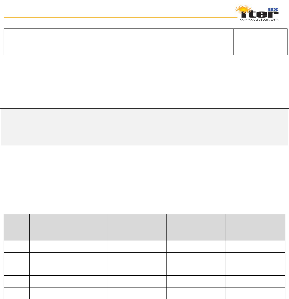
7.1 Hardware
The Company reserves the option to order the maximum quantities listed below or quantities in between
as need but not less than the minimum required as stated. The Company is conducting final testing
components.
Item
No.
Component Name
Test Verification
Quantity
Required
Minimum
Quantity
Required
Company Opt. for
Max Required
1
AFE Board
3
50
90
2
FEAC Board
3
50
100
3
FEAC Daughter Board
3
50
100
4
PM Board
3
50
90
5
PDI Board
3
25
25
Statement of Work for
SVS Custom Electronics PCB Fabrication & Assembly
Page 14 of 14
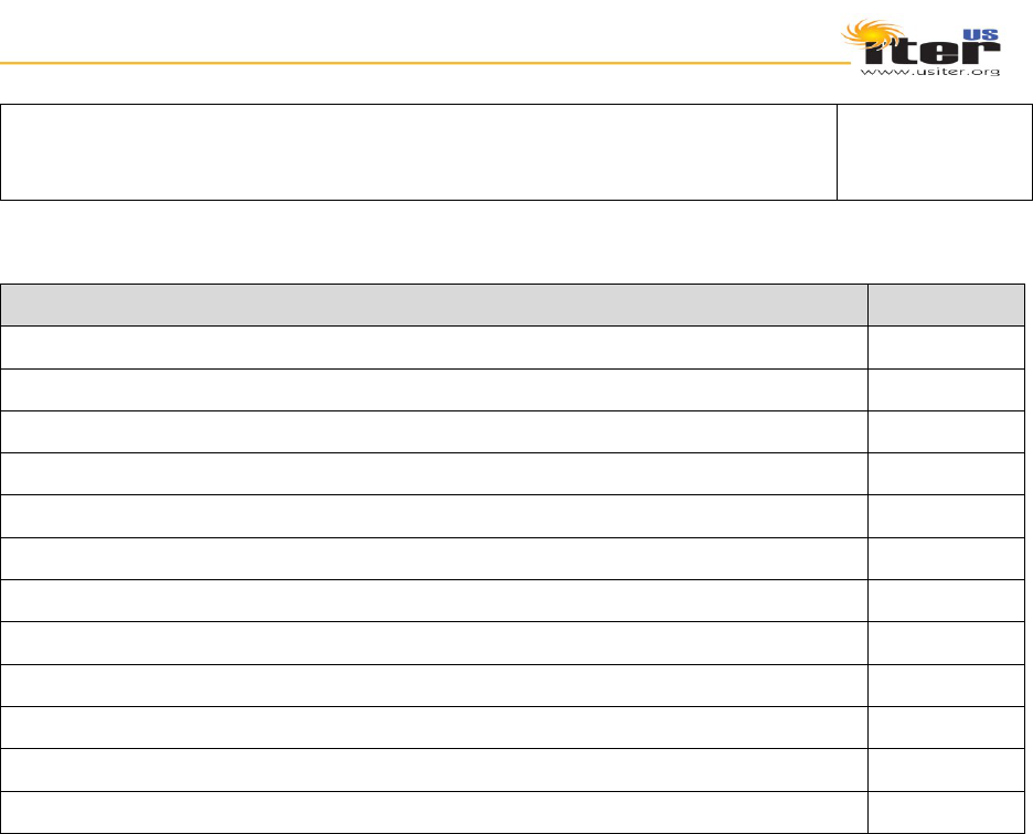
7.2 Documentation
Deliverable
Section
Project Plan
5.1.1
Project Schedule
5.1.1
Kickoff meeting minutes
5.1.2
Progress meeting minutes
5.1.3
Inspection Plan
5.2
Quality Plan
5.3.1
Manufacturing Readiness Review
5.4
Testing
5.6.3
Contractor Release Note(s)
5.7.1
Certificate of Conformity
5.7.2
Manufacturing Dossier
5.8
Shipment Docket
5.9
